← Logic Circuit Simulator Pro Download for PC: Top 6 Simulators in 2024! Download logic circuit simulator pro mod apk latest version (unlocked TDA7294 Multi-Mode PCB: Build a 200W Stereo/Mono Amplifier Easily! tda7294 amplifier circuit →
If you are searching about How to Build a Detailed BOM (Bill of Materials) for PCB Manufacturing you've came to the right place. We have 25 Pictures about How to Build a Detailed BOM (Bill of Materials) for PCB Manufacturing like PCB Designing - How To Design A PCB (Step by Step) | PDF | Printed, ESP32 PSRAM Schematic And Notes PCB Artists, 43% OFF and also Pcb designing how to design a pcb step by step – Artofit. Here it is:
How To Build A Detailed BOM (Bill Of Materials) For PCB Manufacturing
 www.victorypcb.com
How to Build a Detailed BOM (Bill of Materials) for PCB Manufacturing ...
Converting To A Benro Monopod: A Step-by-Step Conversion Guide
 citizenside.com
Converting to a Benro Monopod: A Step-by-Step Conversion Guide ...
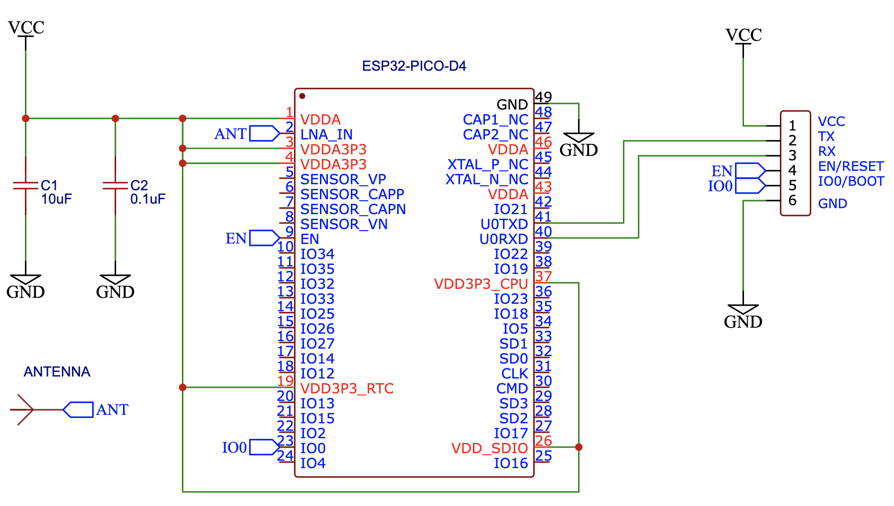
ESP32 PSRAM Schematic And Notes PCB Artists, 43% OFF
 www.pinnaxis.com
ESP32 PSRAM Schematic And Notes PCB Artists, 43% OFF
Pcb Designing How To Design A Pcb Step By Step – Artofit
 www.artofit.org
Pcb designing how to design a pcb step by step – Artofit
Homemade PCB: Step-By-Step Instructions For 2 Methods – Flex PCB
 flexpcb.org
Homemade PCB: Step-By-Step Instructions For 2 Methods – Flex PCB
How Thick Is A Two-layer PCB? Step By Step Guide (2023)ShenZhen Victory
 www.victorypcb.com
How Thick Is A Two-layer PCB? Step By Step Guide (2023)ShenZhen Victory ...
PCB Designing - How To Design A PCB (Step By Step) | PDF | Printed
 www.scribd.com
PCB Designing - How To Design A PCB (Step by Step) | PDF | Printed ...
Pcb Designing How To Design A Pcb Step By Step – Artofit
 www.artofit.org
Pcb designing how to design a pcb step by step – Artofit
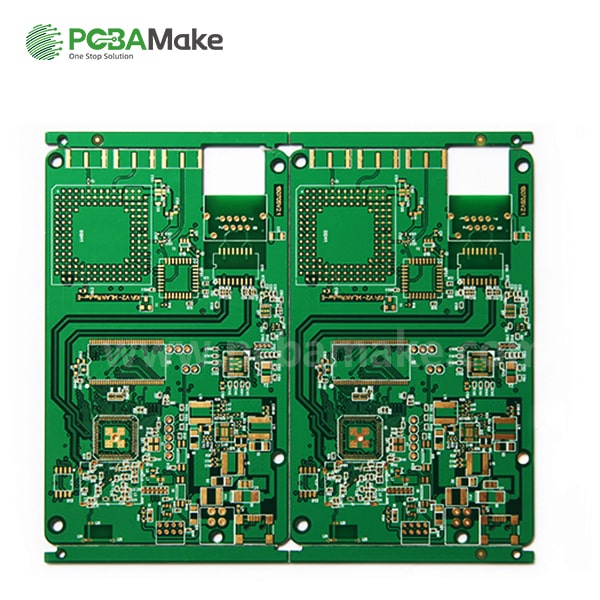
Multilayer PCB-Up To 48 Layers Manufacturing | Advanced Circuits-PcbaMake
 www.pcbamake.com
Multilayer PCB-Up To 48 Layers Manufacturing | Advanced Circuits-PcbaMake
How To 3D Print A Model Of Your PCB | Step By Step
 www.fedevel.com
How To 3D Print a Model of Your PCB | Step by Step
Pcb Designing How To Design A Pcb Step By Step Guide – Artofit
 www.artofit.org
Pcb designing how to design a pcb step by step guide – Artofit
PCB Schematic Diagram Design And Manufacturing Best Practices- Jarnistech
 www.jarnistech.com
PCB Schematic Diagram Design and Manufacturing Best Practices- Jarnistech
Pcb Designing How To Design A Pcb Step By Step – Artofit
 www.artofit.org
Pcb designing how to design a pcb step by step – Artofit
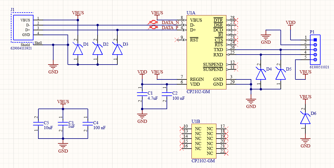
ESP32 CP2102 Programmer Schematic PCB Artists, 58% OFF
 www.elevate.in
ESP32 CP2102 Programmer Schematic PCB Artists, 58% OFF
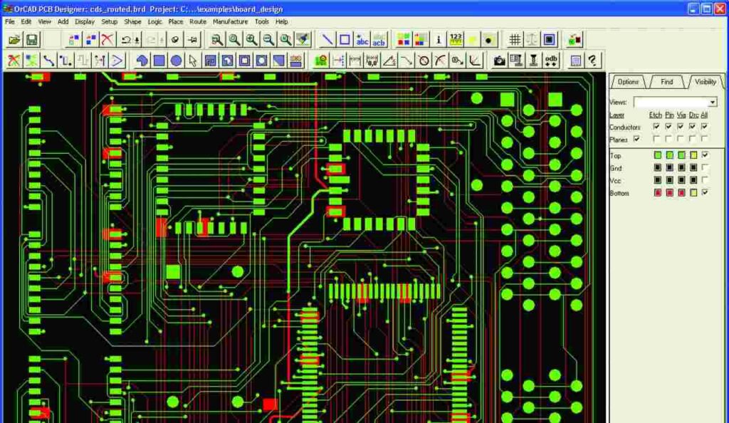
Kicad Update Pcb From Schematic How Too Link An Existing Sch
 diagramudarim5oc.z21.web.core.windows.net
Kicad Update Pcb From Schematic How Too Link An Existing Sch
Pcb Designing How To Design A Pcb Step By Step – Artofit
 www.artofit.org
Pcb designing how to design a pcb step by step – Artofit
10 Steps To Design A GLX PCB Main Schematic
 autoctrls.com
10 Steps to Design a GLX PCB Main Schematic
How To Test For PCB? Step By Step Guide 2023ShenZhen Victory Electronic
 www.victorypcb.com
How To Test For PCB? Step By Step Guide 2023ShenZhen Victory Electronic ...
How To Etch A PCB ? Step By Step - Artist 3D
 artist-3d.com
How to Etch a PCB ? Step by Step - Artist 3D
PCB Schematic Vs. PCB Layout: What's The Difference? - GlobalWellPCBA
 www.globalwellpcba.com
PCB Schematic vs. PCB Layout: What's the Difference? - GlobalWellPCBA
How To Convert Schematic Diagram Into PCB Layout? - Artist 3D
 artist-3d.com
How to Convert Schematic Diagram into PCB layout? - Artist 3D
Protect Your PCB With Potting: A Step-by-Step Guide-TechSparks
 www.tech-sparks.com
Protect Your PCB with Potting: A Step-by-Step Guide-TechSparks
Convert PDF With OCR To Word: Step-by-Step Conversion
 nandbox.com
Convert PDF with OCR to Word: Step-by-Step Conversion
Arduino Uno Schematic Diagram: A Comprehensive Guide
 www.flux.ai
Arduino Uno Schematic Diagram: A Comprehensive Guide
Schematic To Pcb Design
 schematicpartchar.z21.web.core.windows.net
Schematic To Pcb Design
Pcb designing. Pcb designing how to design a pcb step by step – artofit. How to convert schematic diagram into pcb layout?