← iPhone 7 Plus PCB Layout: Schematic Diagram for Repair and Modding! Questions and answers: apple iphone xs 512gb (verizon) mt9d2ll/a iPhone 6 Hardware Solutions: The Ultimate Guide to Repairs and Modifications! Apple análisis del iphone 15 pro max: más potencia de cámara y titanio →
If you are searching about High Speed Pcb Design Guidelines - Design Talk you've visit to the right web. We have 25 Pictures about High Speed Pcb Design Guidelines - Design Talk like Ddr Pcb Layout Guidelines, High Speed Pcb Layout Guidelines - Design Talk and also Interfacing of Nexys 4 DDR board with VGA. | Download Scientific Diagram. Read more:
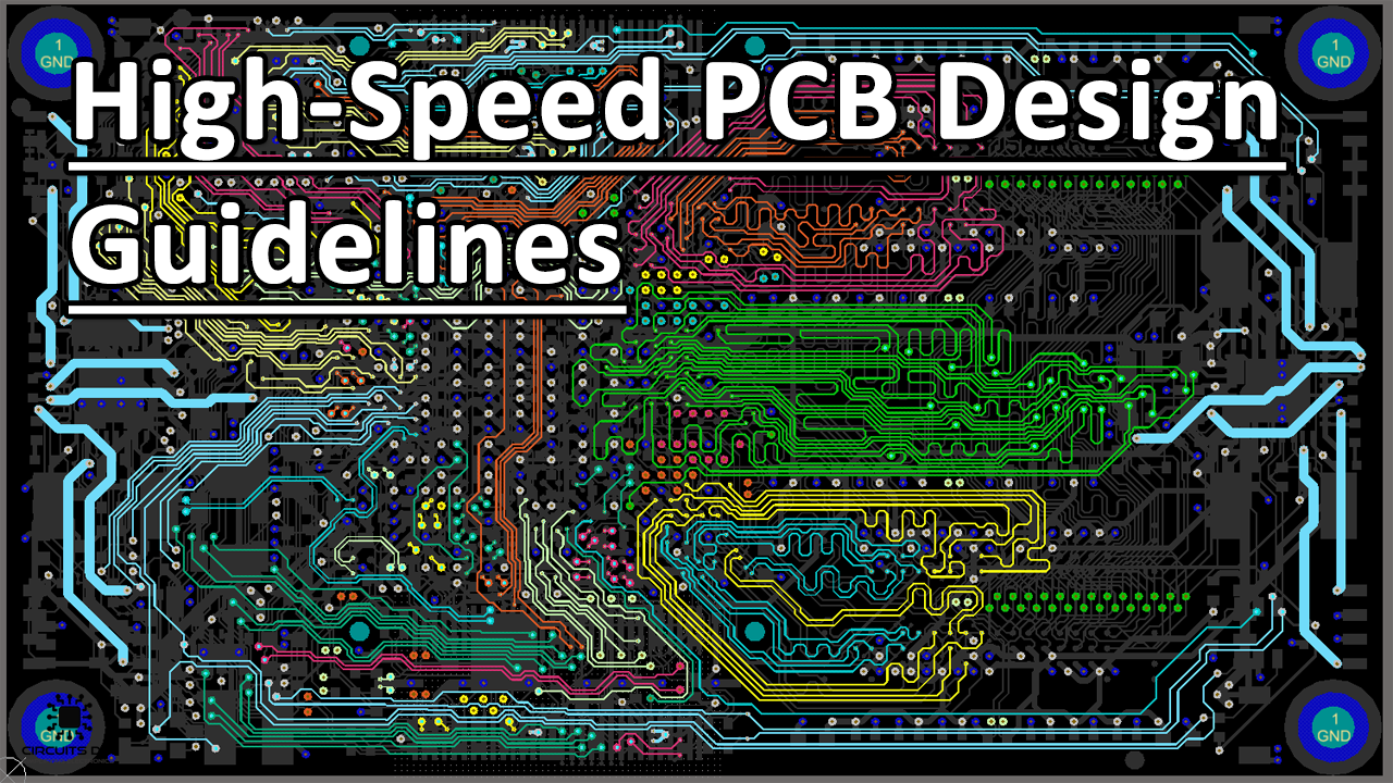
High Speed Pcb Design Guidelines - Design Talk
 design.udlvirtual.edu.pe
High Speed Pcb Design Guidelines - Design Talk
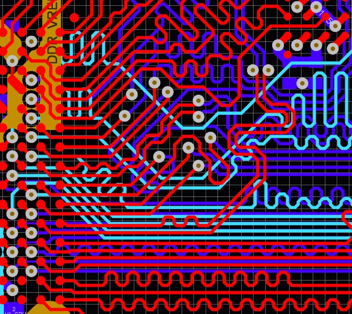
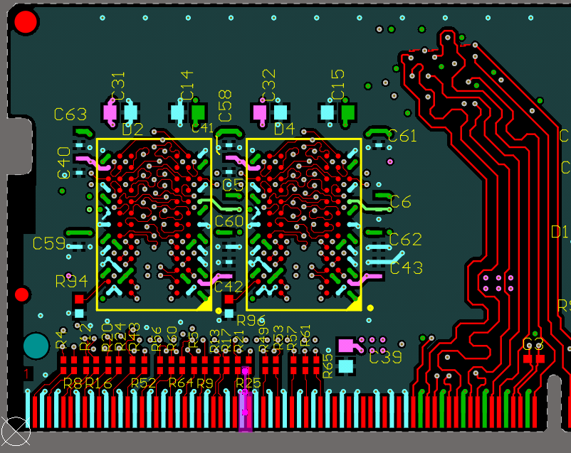
Ddr3 Routing Guidelines And Routing Topologies - Diysica
 diysica.blogspot.com
Ddr3 Routing Guidelines And Routing Topologies - Diysica
Ddr3 Routing Guidelines And Routing Topologies - Diysica
 diysica.blogspot.com
Ddr3 Routing Guidelines And Routing Topologies - Diysica
DDR PHY And Controller | Cadence
 www.cadence.com
DDR PHY and Controller | Cadence
DDR Board Design - New - Micron
 www.yumpu.com
DDR Board Design - New - Micron
Main Design Guidelines & Layout Rules On High Speed PCB
 www.integrasources.com
Main Design Guidelines & Layout Rules on High Speed PCB
Premium Vector | Brand Guidelines Layout And Landscape Logo Brand Book
Premium Vector | Brand guidelines layout and landscape logo brand book ...
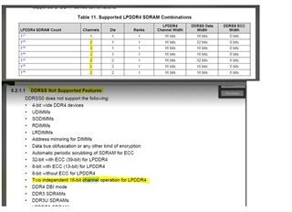
AM6548: DDR Multi-channel And Dual Rank Support - Processors Forum
 e2e.ti.com
AM6548: DDR Multi-channel and Dual Rank Support - Processors forum ...
Interfacing Of Nexys 4 DDR Board With VGA. | Download Scientific Diagram
 www.researchgate.net
Interfacing of Nexys 4 DDR board with VGA. | Download Scientific Diagram
PCB Layout Guidelines.pdf
 www.slideshare.net
PCB Layout guidelines.pdf
Pcb Design Guidelines Mechanical Layer Eurocircuits Eurocircuits Images
 www.tpsearchtool.com
Pcb Design Guidelines Mechanical Layer Eurocircuits Eurocircuits Images
Antenna Wifi Layout At Marcus Lewis Blog
 storage.googleapis.com
Antenna Wifi Layout at Marcus Lewis blog
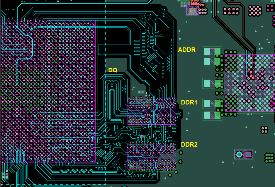
PCB Routing Guidelines For DDR4 Memory Devices And Impedance | Blog
 resources.altium.com
PCB Routing Guidelines for DDR4 Memory Devices and Impedance | Blog ...
FPGA + PCIe Hardware Accelerator Design Walkthrough (DDR3, M.2
 www.fedevel.com
FPGA + PCIe Hardware Accelerator Design Walkthrough (DDR3, M.2 ...
Ddr Pcb Layout Guidelines
 learningmedialiberians.z22.web.core.windows.net
Ddr Pcb Layout Guidelines
PCB Routing Guidelines For DDR4 Memory Devices And Impedance | Blog
 resources.altium.com
PCB Routing Guidelines for DDR4 Memory Devices and Impedance | Blog ...
Ddr Board Chip Macro Image Of Modern Hightech Technologies Stock Photo
 www.istockphoto.com
Ddr Board Chip Macro Image Of Modern Hightech Technologies Stock Photo ...
High Speed Pcb Layout Guidelines - Design Talk
 design.udlvirtual.edu.pe
High Speed Pcb Layout Guidelines - Design Talk
DDR TI Guidelines | PDF | Capacitor | Manufactured Goods
 www.scribd.com
DDR TI Guidelines | PDF | Capacitor | Manufactured Goods
Wedding Board Decoration | Personalised Engagement Board
 homafy.com
Wedding Board Decoration | Personalised Engagement Board
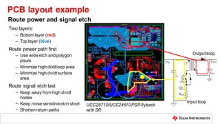
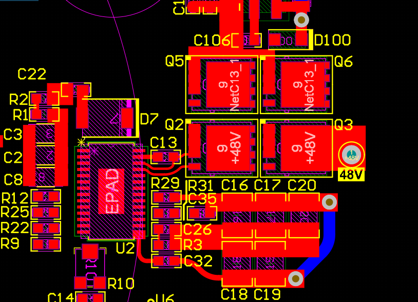
Switched-Mode Power Supply PCB Design Guidelines | Altium
 resources.altium.com
Switched-Mode Power Supply PCB Design Guidelines | Altium
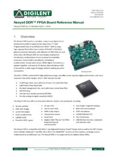
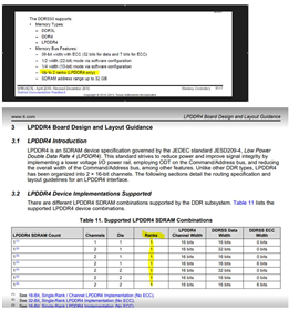
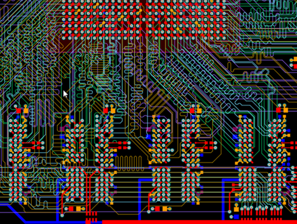
Nexys4 DDR™ FPGA Board Reference Manual - Digilentinc / Nexys4-ddr-fpga
 pdf4pro.com
Nexys4 DDR™ FPGA Board Reference Manual - Digilentinc / nexys4-ddr-fpga ...
AM6548: DDR Multi-channel And Dual Rank Support - Processors Forum
 e2e.ti.com
AM6548: DDR Multi-channel and Dual Rank Support - Processors forum ...
Using SDRAM Vs. DDR RAM In Your PCB Design | Blog | Altium Designer
 resources.altium.com
Using SDRAM vs. DDR RAM in Your PCB Design | Blog | Altium Designer
Top 5 Pcb Design Guidelines In Electronics Industry 2 - Vrogue.co
 www.vrogue.co
Top 5 Pcb Design Guidelines In Electronics Industry 2 - vrogue.co
Ddr3 routing guidelines and routing topologies. ddr ti guidelines. Ddr pcb layout guidelines